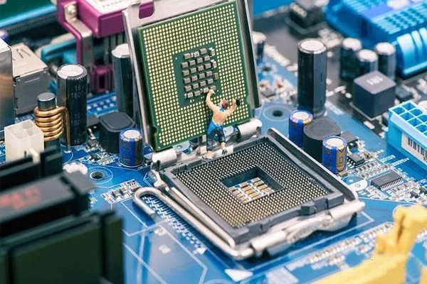
Semiconductor material refers to the material whose conductivity is between metal and insulator. The conductivity of semiconductor material is between Euro / cm. In general, the conductivity increases with the increase of temperature. Semiconductor materials are important materials for making transistors, integrated circuits, power electronic devices, and optoelectronic devices.
The semiconductor materials market can be divided into wafer materials and packaging materials markets. Among them, the wafer materials mainly include silicon wafers, photomasks, photoresists, photoresist auxiliary equipment, wet processes, sputtering targets, polishing solutions, and other materials. Packaging materials are mainly laminated substrates, lead frames, bonding wires, molding compounds, underfills, liquid sealants, die attach materials, solder balls, wafer-level packaging media, and thermal interface materials.
Low self-sufficiency in semiconductor materials
In the field of semiconductor materials, due to high technical barriers to high-end products and insufficient long-term R & D investment and accumulation by domestic companies, China's semiconductor materials are mostly in the low-end area in the international division of labor. For example, the top six companies in the global wafer market have a market share of over 90%, the top five companies in the photoresist global market have a market share of over 80%, and the top six companies in the high-purity reagent global market have a market share of 80%. Above, the top seven companies in the global market for CMP materials have a market share of 90%.
The self-sufficiency rate of most domestic products is low, basically less than 30%, and most of them are packaging materials with low technical barriers. The localization ratio of wafer manufacturing materials is lower, which mainly depends on imports. In addition, domestic semiconductor material companies focus on production lines below 6 inches. At present, a few manufacturers have begun to enter domestic 8-inch and 12-inch production lines.
Large silicon wafers: Silicon wafers, also called silicon wafers, are the most important semiconductor materials. They mainly include polished wafers, annealed wafers, epitaxial wafers, segment spacers, and silicon wafers on insulators. Polished wafers are the most used products. Silicon wafer products are also produced by secondary processing on the basis of polished wafers. The sales of silicon wafers account for 32% to 40% of the total sales of the semiconductor materials market.
Silicon wafer diameters are mainly 3 inches, 4 inches, 6 inches, 8 inches, 12 inches (300mm), and currently have developed to 18 inches (450mm) and other specifications. The larger the diameter, the greater the number of integrated circuit chips that can be made in a single process cycle on a silicon wafer, and the lower the cost of each chip. Therefore, larger-diameter silicon wafers are the development direction of various wafer-making technologies. But the larger the size of the silicon wafer, the higher the requirements for microelectronics process design, materials, and technology.
Silicon wafers have extremely high technical barriers, and the global market is showing an oligopoly pattern. Shin-Etsu and SUMCO (combined by Mitsubishi Silicon Materials and Sumitomo Materials Sitix Division) have always occupied major market shares, each accounting for about 30%. , Other major companies are Germany Siltroni (a subsidiary of German chemical company Wacker), South Korea LGSiltron, the United States MEMC and Taiwan Sino-US silicon crystal products SAS four companies. The above six suppliers together account for more than 90% of the global market share.

 Your location: